

Aid in RF Circuit Board Design
RF circuit boards are the backbone of many modern communication technologies, including mobile phones, radar systems, GPS devices, and wireless networks. They operate at high frequencies that demand meticulous design and specific materials to ensure signal integrity and minimize loss. These high-performance boards are also subject to complex manufacturing and testing processes to ensure the PCB performs as intended. The ability to quickly design, test, and refine RF circuit board designs with the help of automated machines is a key factor in ensuring these complex electronics meet their performance goals.
Often, RF circuits use multi-layer PCBs with specialized laminates to meet their unique electrical requirements. These laminates can be expensive, so it is important to choose the right ones for each application. An RF engineer will need to evaluate the dielectric constant (eR) of each layer in the stack-up to select the right material for the job. An RF engineer will also need to determine the best layout for the components in the RF circuit board to reduce the length of signals that need to travel, thereby decreasing their transmission losses and minimizing cross-talk between the components.
As part of the design process, RF engineers will conduct simulations to predict how the RF circuit board will perform after it is produced and in operation. This includes RF-specific tests such as S-parameters to measure the impedance uniformity of each layer, and time-domain reflectometry to identify impedance mismatches, signal reflections, and other anomalies. These tests will provide valuable feedback to the RF engineer on how to improve the design in order to meet the desired performance criteria before it goes into production.
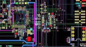
Automated Machines Aid in RF Circuit Board Design
In addition to these testing techniques, RF engineers will likely need to utilize simulation software to iteratively test and improve their designs. This can include adjusting trace widths and spacing, changing the RF PCB layer stack-up, or even repositioning components on the RF circuit board to optimize signal isolation. These iterative changes can make a significant difference in reducing signal loss, improving impedance matching, and mitigating noise sources.
The specialized layers in a rf circuit board design are typically divided into sections for RF, non-RF, power, and ground planes. In most cases, the RF components and traces are placed on the top layer followed by a ground plane and power planes. This arrangement provides minimal interference between RF and non-RF components and traces and offers the best performance and ground return current path. In addition, it is never good to place an RF trace and a normal PCB trace parallel to each other as this can cause significant attenuation.
The specialized nature of an RF circuit board demands careful consideration in every step of the design and production process. Working with a professional RF engineering firm can help ensure that all aspects of the RF circuit board will meet or exceed the performance expectations of the final product. This will require careful collaboration between the RF design team and the PCB manufacturer to address manufacturing and testing requirements.


